
In the world of electronics manufacturing, Gerber files are the standard for describing the layers of a printed circuit board (PCB). They are essentially the blueprints that guide the fabrication process. However, there are times when you might only have the Gerber files and need to reconstruct the original PCB design, a process often referred to as reverse engineering. This guide will walk you through the detailed steps of converting Gerber files back into a usable PCB layout, a valuable skill for any electronics engineer. For professional assistance with this process, you can always consult experts like those at www.fastpcbreverse.com.
The Step-by-Step Conversion Process
While there are various tools available, this guide will focus on the general process using a CAM (Computer-Aided Manufacturing) tool, with examples that are conceptually similar to what you would find in software like Altium Designer’s Camtastic.
Step 1: Create a New CAM Document
The first step is to open your CAM software and create a new CAM document. This will be the workspace where you import and process the Gerber files.

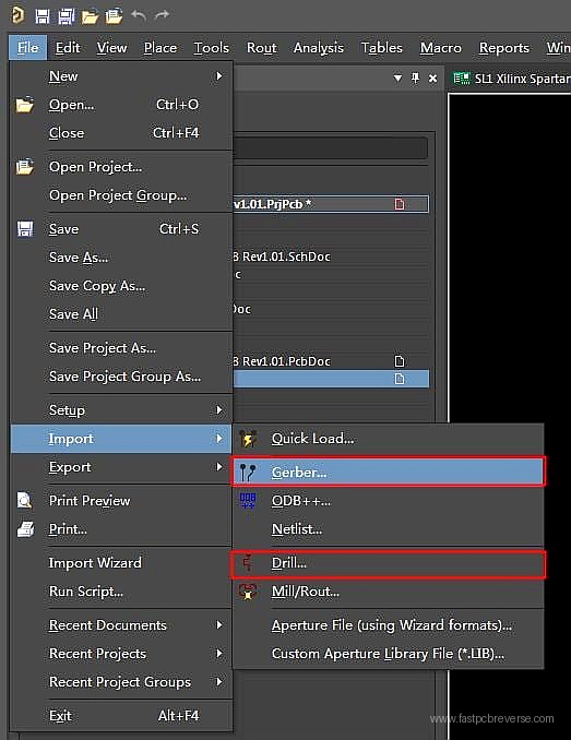
Step 2: Import Gerber and NC Drill Files
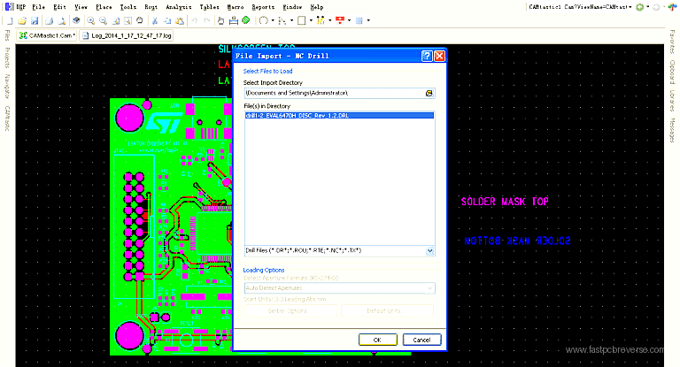
This is a critical stage. You must import not only the Gerber files for each layer of the PCB but also the NC (Numeric Control) Drill files. The drill files contain the information about the size and location of all the holes to be drilled in the board. Without them, you won’t have a complete picture of the PCB’s structure, and you won’t be able to extract a correct netlist.
For easier identification, you can often define the file extensions that your CAM tool recognizes for different types of Gerber and drill files.

Once imported, you can view the individual layers in your CAM editor.

Step 3: Layer Mapping
After importing the files, you need to map each Gerber layer to its corresponding layer in the PCB stackup. This is another crucial step where precision is key. You’ll need to correctly identify and map the top and bottom copper layers, any internal signal or plane layers, the solder mask layers, and the silkscreen layers. The NC Drill file also needs to be mapped to the drill layers

Step 4: Define the Layer Order
With the layers mapped, the next step is to define their physical order in the PCB stackup. The top layer is typically assigned the first position, and the subsequent layers follow the actual physical structure of the board. It’s important to get this right, especially if the board has blind or buried vias, as an incorrect layer order will lead to errors when you export the final PCB file.

Step 5: Extract the Netlist
If the previous steps have been completed correctly, your CAM tool should now be able to deduce the netlist from the imported data. The netlist describes the electrical connections between the components on the board. You can usually find an
option to extract the netlist in the tools menu.

Step 6: Export the PCB Layout
The final step is to export the complete design as a PCB layout file. If the netlist or other critical information is missing, this option may be unavailable or grayed out. A successful export will provide you with a complete PCB file that you can then open in your preferred PCB design software for further editing or analysis.

Conclusion
Converting Gerber files back to a PCB layout is a meticulous process that requires attention to detail at every step. By carefully following the procedures for importing, mapping, and ordering the layers, and then extracting the netlist, you can successfully reverse-engineer a PCB design from its manufacturing files. This process is invaluable for tasks such as legacy product support, competitive analysis, or when original design files have been lost. For complex projects or if you require professional reverse engineering services, consider reaching out to the experts at www.fastpcbreverse.com.