
In the world of electronics, the Printed Circuit Board (PCB) is the foundation upon which all components are mounted and interconnected. Before a physical PCB can be manufactured, a detailed blueprint must be created. This blueprint is the PCB schematic, a graphical representation of the electronic circuit. A well-designed schematic is crucial for a successful and functional electronic device. This guide, brought to you by FASTPCBREVERSE, will walk you through the essential steps of creating a professional PCB schematic.
The Importance of a Good Schematic
A PCB schematic is more than just a drawing; it is the master plan for your electronic circuit. It defines the components to be used, their interconnections, and the overall functionality of the device. A clear, accurate, and well-documented schematic serves several critical purposes:
•Design Verification: It allows engineers to review and verify the circuit design before moving to the layout stage.
•Collaboration: It provides a common language for design teams to collaborate effectively.
•Troubleshooting and Debugging: A good schematic is an invaluable tool for identifying and resolving issues during testing and in the final product.
•Manufacturing: It serves as the primary reference for the PCB layout and assembly processes.
At FASTPCBREVERSE, we understand that a high-quality schematic is the cornerstone of a successful PCB project. Our expertise in PCB reverse engineering and design has shown us time and again that a meticulous approach to schematic creation saves time, reduces costs, and results in a more reliable product.
Step 1: Conceptualization and Circuit Design
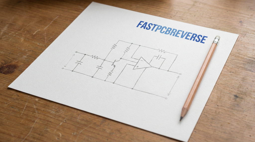
The first step in creating a PCB schematic is to have a clear understanding of the circuit you want to build. This involves defining the functionality of the device and creating a preliminary circuit diagram. This initial diagram can be a simple hand-drawn sketch or a more formal drawing created with basic drawing software. The goal is to outline the main functional blocks of the circuit and the flow of signals between them.
During this phase, you should consider:
•The overall purpose of the device.
•The required inputs and outputs.
•The power requirements.
•Any specific performance criteria, such as speed, power consumption, or size constraints.
This conceptual design will serve as the basis for the detailed schematic you will create in the next step.
Step 2: Schematic Capture with EDA Software
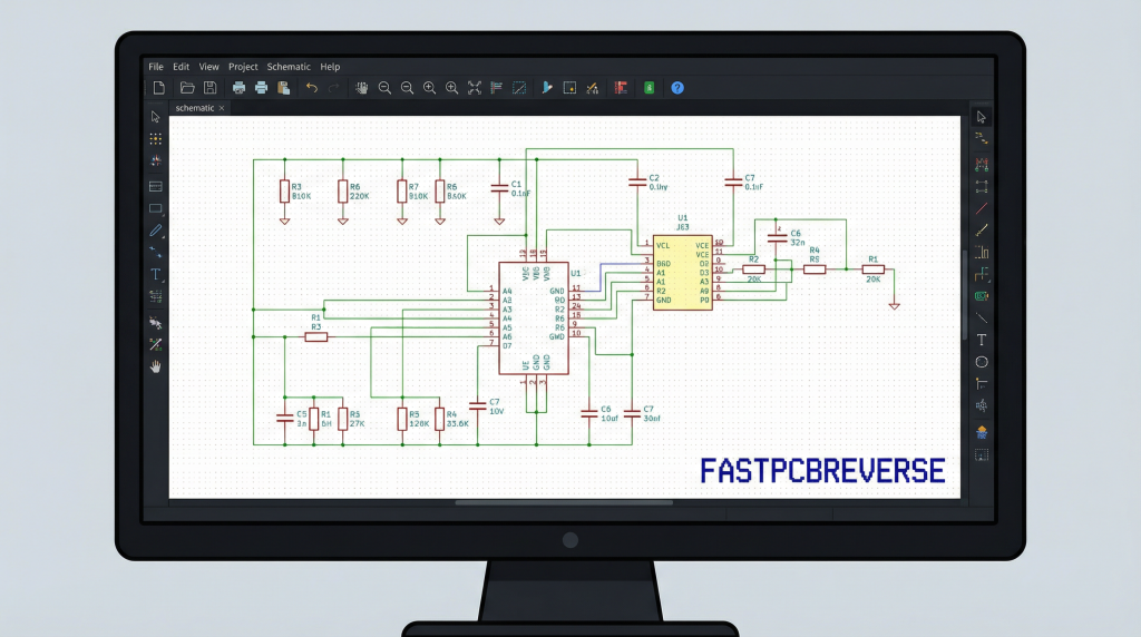
Once you have a solid conceptual design, it’s time to translate it into a formal schematic using Electronic Design Automation (EDA) software. EDA software provides a specialized environment for creating, editing, and verifying electronic schematics. There are many EDA tools available, ranging from free and open-source options like KiCad to powerful commercial packages like Altium Designer and Cadence Allegro.
The process of schematic capture involves placing symbols for each component in your circuit and then drawing wires to represent the electrical connections between them. Each component symbol is a graphical representation of a physical component, and it contains important information such as the component’s name, value, and footprint.
When creating your schematic, it is essential to maintain a clear and organized structure. This can be achieved by:
•Using a consistent naming convention for components and nets.
•Grouping related components together to create logical blocks.
•Using net labels to simplify complex wiring and improve readability.
•Adding comments and notes to explain the functionality of different parts of the circuit.
FASTPCBREVERSE has extensive experience working with various EDA tools and can assist you in creating clean, well-documented schematics that are optimized for manufacturability.
Step 3: Component Selection and Footprint Assignment
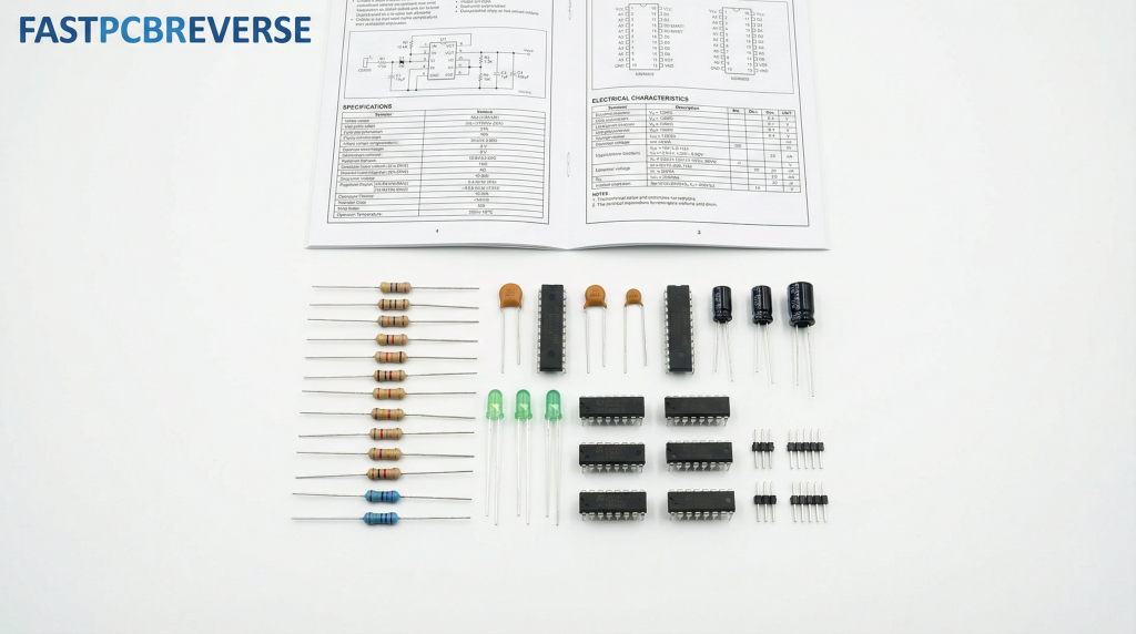
As you create your schematic, you will need to select the specific electronic components that will be used in your design. This involves choosing components that meet the performance requirements of your circuit while also considering factors such as cost, availability, and size.
Once you have selected a component, you must assign the correct footprint to its symbol in the schematic. The footprint is a drawing of the physical pads or holes on the PCB where the component will be soldered. It is crucial to select the correct footprint for each component, as an incorrect footprint will result in a PCB that cannot be assembled.
Most EDA software includes extensive libraries of component symbols and footprints. However, you may occasionally need to create custom symbols and footprints for unique or specialized components. When creating custom library parts, it is essential to follow the manufacturer’s datasheet specifications carefully to ensure accuracy.
Step 4: Wiring and Netlisting
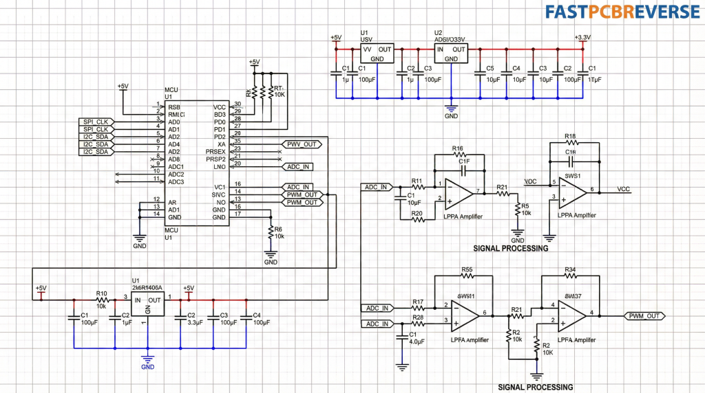
With all the components placed and their footprints assigned, the next step is to wire them together according to your circuit diagram. This is done by drawing lines, called nets, between the pins of the component symbols. As you draw the nets, the EDA software will automatically keep track of the connections and create a netlist.
The netlist is a text-based file that describes all the components and their interconnections in the schematic. It is a critical file that will be used in the next stage of the PCB design process: the PCB layout.
Step 5: Verification and Error Checking
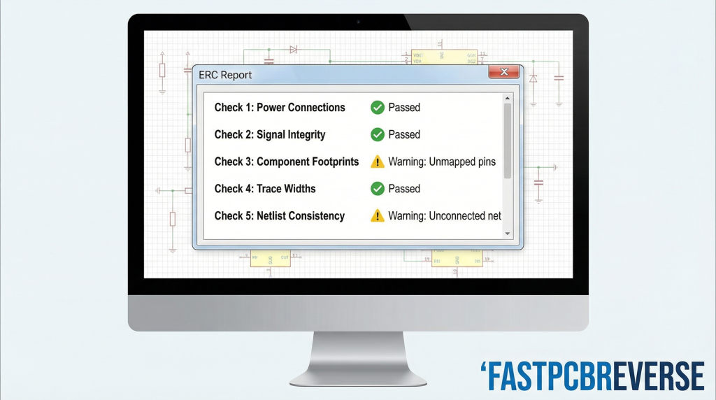
Before you can move on to the PCB layout, it is essential to verify your schematic for errors. All EDA software includes a tool called the Electrical Rule Checker (ERC), which can automatically check your schematic for common errors such as:
•Unconnected pins.
•Outputs connected together.
•Short circuits between power and ground.
•Incorrectly labeled nets.
Running the ERC and carefully reviewing any reported errors is a critical step in ensuring the integrity of your design. It is much easier and less costly to fix errors at the schematic stage than it is to correct them after the PCB has been manufactured.
In addition to running the ERC, it is also a good practice to manually review your schematic one last time. Check for any logical errors or design flaws that the ERC may not have caught. A peer review by another engineer can also be extremely valuable in catching potential issues.
Creating a PCB schematic is a meticulous but rewarding process. A well-designed schematic is the foundation of a successful electronic product, and it is a skill that every electronics engineer should master. By following the steps outlined in this guide, you can create clear, accurate, and manufacturable PCB schematics.
At FASTPCBREVERSE, we are committed to helping our clients achieve their design goals. Whether you need assistance with schematic capture, component selection, or design verification, our team of experienced engineers is here to help. Contact us today to learn more about our PCB design and reverse engineering services.